Daijiworld Media Network - Bhubaneswar
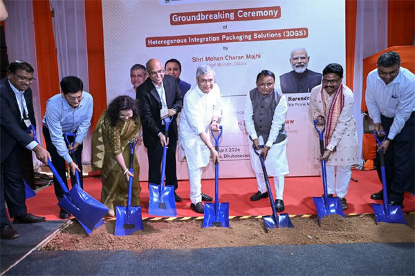
Bhubaneswar, Apr 19: Odisha has taken a major step toward becoming a key hub in India’s semiconductor ecosystem with the foundation laying of the country’s first advanced 3D glass substrate packaging facility by 3D Glass Solutions at Infovally in Bhubaneswar.
The project was inaugurated in the presence of Odisha Chief Minister Mohan Charan Majhi, Union Electronics and IT Minister Ashwini Vaishnaw, and Odisha Electronics and IT Minister Dr. Mukesh Mahaling.
The facility, backed by an investment of around Rs 2,000 crore, is expected to manufacture nearly 70,000 glass panels annually, along with 50 million assembled units and 13,200 advanced 3DHI modules. Officials estimate that the project will generate approximately 2,500 direct and indirect employment opportunities.
Speaking at the event, Chief Minister Majhi said the initiative marks not only a milestone for Odisha but also a significant advancement in India’s technological journey. He highlighted that the facility will produce cutting-edge components essential for sectors such as artificial intelligence, high-performance computing, and defence electronics.
Majhi said Odisha is fast emerging as a preferred destination for semiconductor investments, citing its natural resources, skilled workforce, infrastructure development, connectivity, and investor-friendly governance. He added that the state aims to position itself as a key driver in the vision of Atmanirbhar Bharat under the leadership of Prime Minister Narendra Modi.
Encouraging young people, the Chief Minister described the project as a “golden opportunity” for students and engineers in Odisha to acquire skills and enter the growing semiconductor sector.
He also noted that semiconductor-related investments in the state have already crossed Rs 10,000 crore, with companies such as RIR Power Electronics and SiCSem establishing operations in Odisha.
Union Minister Vaishnaw said the initiative will accelerate industrial growth in the state and help transform Odisha into a major IT and semiconductor hub. He added that the new facility will introduce first-of-its-kind technology in India and play a key role in shaping the future of the semiconductor industry.